I recently got hold of this retro looking instrument lamp as a freebie from a local share group:

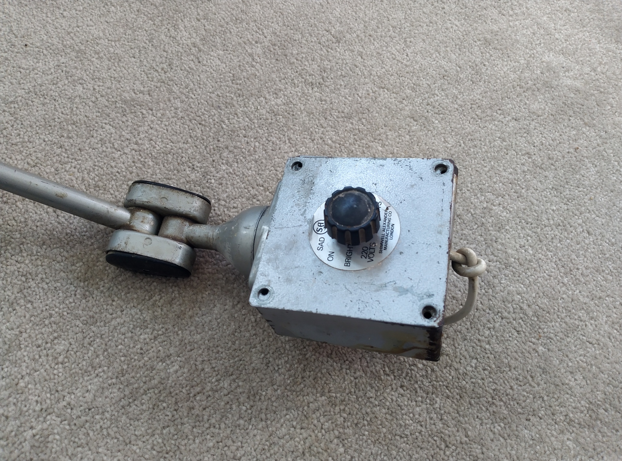
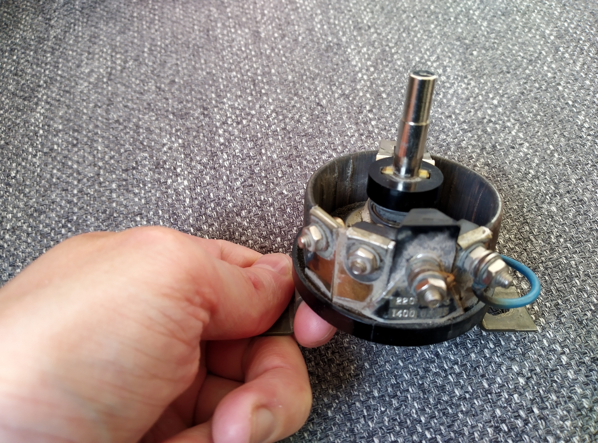
It’s a little bit tatty and the dimmer didn’t work but I thought it seemed like a great opportunity for a project. Opening it up, I found that the dimmer was actually just a wirewound variable resistor. It seemed like there was a break in the resistance wire somewhere, which would explain why the lamp wouldn’t work.
I had a think about what to do with this project. I decided that I’d like to change it to use LEDs, and create a new dimmer. But what kind of LEDs? Something on my todo list for someday is to actually design my own LED board, so I know I’m using emitters with high CRI and the thermal management is good. But I decided that that wasn’t a task for this project, and using a filament LED bulb would give it more character, and be less custom circuitry to maintain and debug.
Dimming
The problem with using an off-the-shelf LED bulb is the dimming: if you’ve ever tried using a supposedly “dimmable” LED bulb with a conventional TRIAC dimmer, you’ll know that the results can be hit-and-miss. As far as I’m aware, the main reason for this is that the current consumption of an LED bulb is typically below the hold current of a TRIAC. Take the BT137 for example. It has a typical hold current of 2.5mA, which corresponds to 0.6W at 230V. But it could be as high as 20mA, corresponding to about 5W. With a load smaller than the hold current, the TRIAC will switch off, only to be triggered again once sufficient voltage develops across the gate circuitry. And this will result in the all-too-familiar annoying buzzing, and probably flickering too. So for LEDs, TRIAC dimmers are out.
But why trailing edge?
That explains why we can’t use a TRIAC as the switching element of a phase-control dimmer. But why is it commonly said that trailing edge dimmers are preferred over leading edge for LEDs?
To be honest, I’m not entirely sure. I suspect this is a comparatively minor optimisation. A reason I’ve heard alluded to but not explicitly discussed in any detail is that the sharp leading edge can cause some unspecified problems. I’m not sure if this is current stresses affecting reliability, or high dI/dt causing audible noise in magnetic components. I’d hazard a guess that step one in development of LED dimmers was that TRIACs were abandoned in favour of back to back MOSFETs, and so more complex control circuitry (probably microcontroller based) was required. And once you’re using a microcontroller anyway, you may as well use trailing edge dimming to avoid the current spike on the leading edge too!
One other possibility I considered was, since most LED bulbs will have rectification and smoothing, does trailing edge dimming give finer control over average rectified voltage? The answer is, not really. The animations below show a simulation of a leading-edge and trailing-edge dimmed signal, a full-wave rectified DC voltage produced from that, and the average voltage.

In both cases, the average DC voltage essentially just follows the peak of the waveform, and so the DC voltage increases in a comparable way. The variation in average DC voltage with phase angle is plotted here:
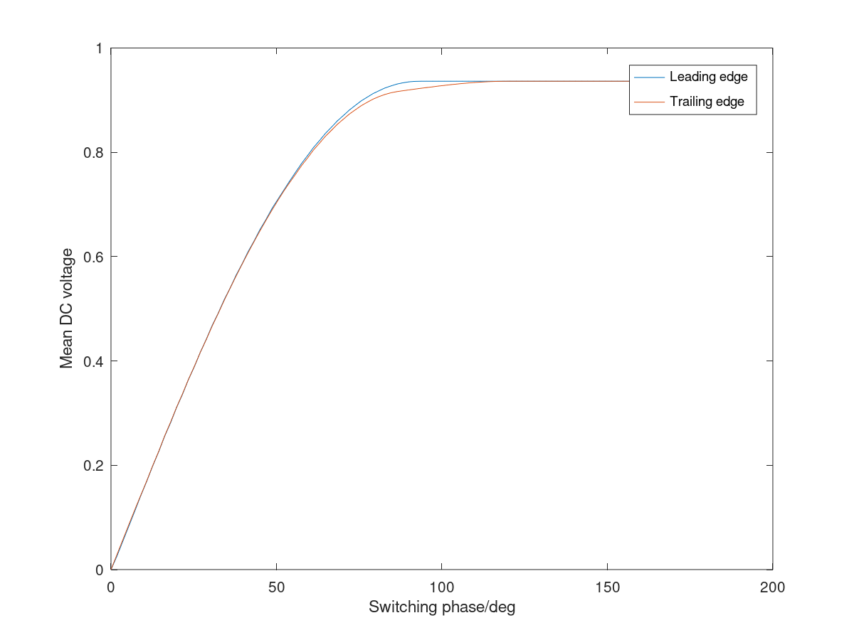
As you’d expect, after 90 degrees there’s essentially no further increase, as the peak of the AC waveform is already being rectified. There’s a very slight variation due to a small difference in droop between the two cases.
That’s as much as I’m going to say on the motivation behind trailing edge dimmers, but if you want to see some practical examples, John Ward has a demonstration of a few on his youtube channel.
Implementation
Having decided to use a trailing edge dimmer, the next question was how to do it. The obvious option is to just buy or adapt something off-the shelf. Since the dimmer unit on the lamp is slightly larger than a standard pattress box, it should be possible to adapt a standard wall-mounting dimmer switch. This would probably have been the cheapest and easiest solution, but off-the-shelf dimmer switches still aren’t cheap enough to put me off having some fun by designing my own.
As far as designing my own is concerned, there seem to be three options: the easiest is to use a dimmer IC, such as Fairchild’s FL5150. It seems like a nice integrated solution and GreatScott! did a PCB layout using it. The second option would be to make a microcontroller circuit: essentially digitising a potentiometer input, synchronising to the mains switching and producing a pulse to turn on the back-to-back MOSFETs. Again, in the same video above, GreatScott! does exactly that. I didn’t choose either of these options though. The FL5150 wasn’t in stock on LCSC and I couldn’t be bothered to look elsewhere. I didn’t want to use a microcontroller because there’s pretty much nothing I enjoy about working with microcontrollers: installing development environments, finding where I put my programmer, writing and debugging code, fixing problems with device or programmer detection. All of these things make me want to cry and I’d rather be doing some analog electronic design.
So that’s what I decided to do: create a dimmer circuit in analog electronics. I figured this would nicely complement the two approaches GreatScott! had already explored too.
Circuit Block Diagram
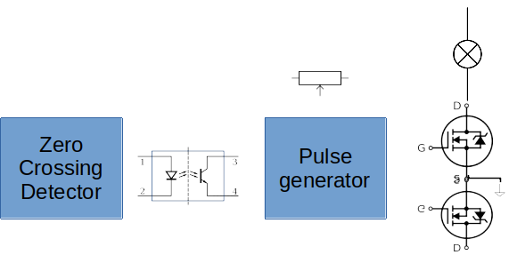
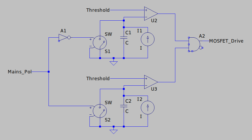
The general idea for this circuit is that the light bulb current will be switched on or off by two back-to-back MOSFETs to give bidirectional current control. These will be driven by a pulse generator with a potentiometer to provide the setpoint, and that will rely on a zero-crossing detector for the mains voltage.
The frustrating thing is, I couldn’t think of a way to implement this without an optoisolator in the middle. The pulse generator circuit needs to produce an output referenced to the common source of the MOSFETs. However, such a circuit wouldn’t be able to see every mains voltage transition, since it can only see the mains voltage when one or other of the MOSFETs is switched on (which won’t be the case at a transition, except at 100% output), or a body diode is forward biased. And if we rely on this, depending on which body diode we’re using we might see the (unknown) voltage drop across the load in addition to the forward voltage. The FL5150 IC seems to achieve this, unless it’s secretly using some kind of capacitive isolator, but I couldn’t figure out how so I’m stuck with the optoisolator.
Zero-Crossing Detector
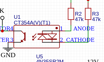
The simplest way to achieve the zero-crossing detection would have just been to place the optocoupler across the supply either to detect its polarity or, as GreatScott! did, use an optoisolator with reverse-parallel emitters to produce a “blip” at a zero-crossing. The problem with this is that there’s a tradeoff between the phase accuracy and power dissipation – and a hard limit on the latter imposed by the optocoupler.
Here, he’s chosen 100kohm of series resistance. That gives a maximum current of around 3.3mA with 230VAC. But the current transfer ratio is around 100%, meaning that, assuming a 10kohm pullup inside the ATTiny and a ~2.5V threshold, about 250uA needs to flow to cause a transition, which corresponds to a voltage of around 25V across the mains supply. So the transition will happen typically ~25V either side of the threshold. This will give a phase error of typically about asin(25*sqrt(2)/230)=9 degrees, which isn’t good enough for my liking! If the optocoupler transfer ratio is at its minimum of 50%, the phase error will be even worse. Plus, this circuit is burning around about 230V*230V/100k = 0.5W, which is rather a lot of energy to waste when we’ll only be dimming a <10W bulb!
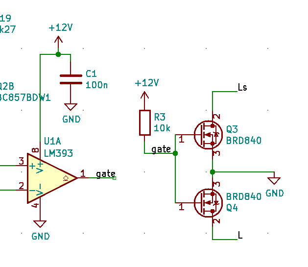
My choice of circuit uses a comparator to give a precise transition. An LM393 clone is used simply because it was the cheapest dual comparator on LCSC and I need a dual comparator later on. The RC network on the input biases the comparator inputs within the common mode range of the comparator, and then detects the polarity of the AC component. It should be obvious that both comparator inputs will see the same DC component (give or take input bias currents*100kohm) – simply ignore anything left of the capacitor since no DC current will flow through here. So both comparator inputs will be biased at 2.5V.
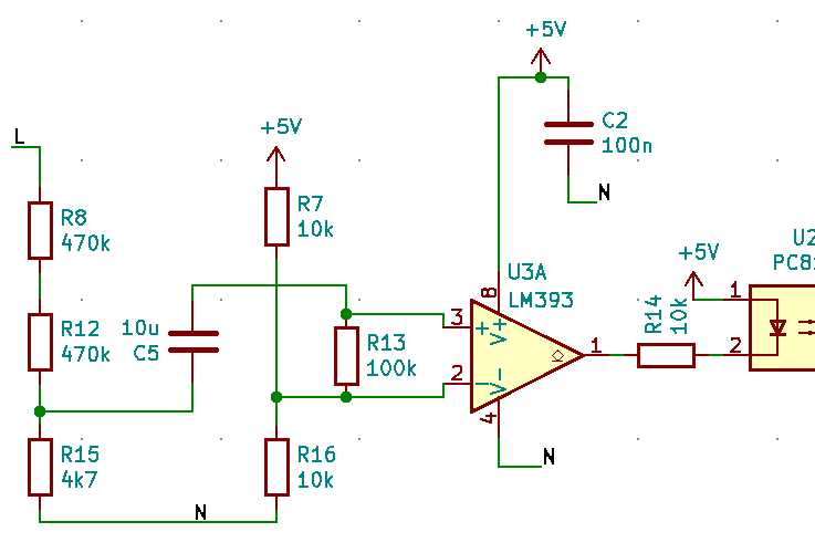
For the AC component, we can treat C5 as a short circuit since the impedance at 50Hz is just 318 ohms. This gives a thévenin equivalent circuit thus:
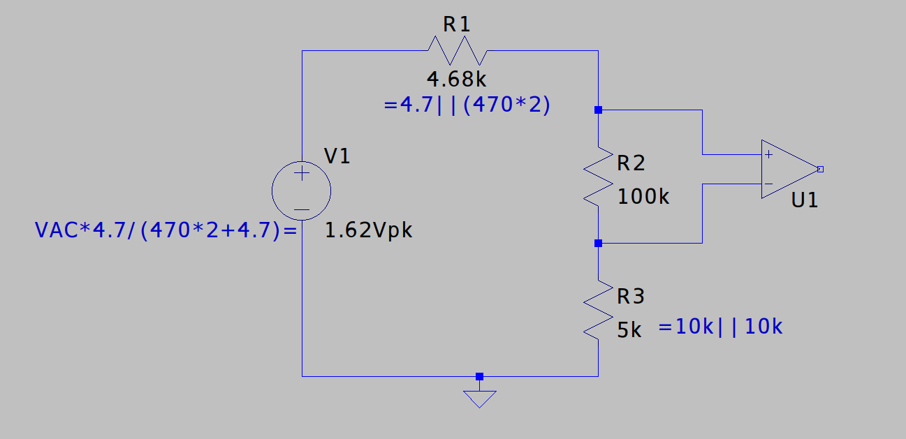
From this we can see that the majority of the 1.62V peak AC will be seen across the comparator input. The comparator is specified to have an input offset voltage of +/-5mV max, and is specified to have a negligible (~1us) switching time with 5mV overdrive, so it should trigger within arcsin(10mV/1.62V) = 0.35 degrees of the line transition. Another source of error is the phase shift of the RC network. Bringing the 318 ohms impedance of the capacitor back in, this will mean the impedance of this circuit is at an angle of atan(0.318k/(100k+5k+4.68k))=0.16 degrees. So in total, this circuit indicates the phase of the AC line signal with about 0.51 degrees of phase error.
The more pedantic might point out that this isn’t really a zero-crossing detector: just a polarity detector!
Pulse Generator
After the optoisolator (just selected as the cheapest one available on LCSC!), we need a pulse generator. This needs to produce a pulse on each change of AC signal polarity, of a duration set by the position of a potentiometer. For this, I’ll charge a capacitor at each transition and turn off the MOSFET when we reach the threshold set by the potentiometer. I figured I’ll use two circuits like this, operating out of phase:
Timing Capacitor
In this circuit, we don’t want to use currents which are too low, otherwise leakages become an issue. But we also want to keep the capacitance low enough to allow us to use a precision type.
The circuit is going to be running off 12V (for reasons I’ll explain later), and I want the capacitor to charge up to half the supply voltage (to keep within the common mode range of the comparator) within half a mains cycle. With our mains frequency of 50Hz, this means that dV/dt=6V*50Hz*2=600V/s. Since dV/dt=I/C, this gives us the relationship between the current setpoint and the capacitance. I selected 100nF and 60uA. 60uA is low enough that the leakage of most components isn’t significant, while 100nF is the largest value I could get in 1206 C0G (a class 1 dielectric).
I could have stretched to far higher capacitances with an X7R capacitor but let’s look at the specs for, say, an AVX 10uF 25V 1206 capacitor:
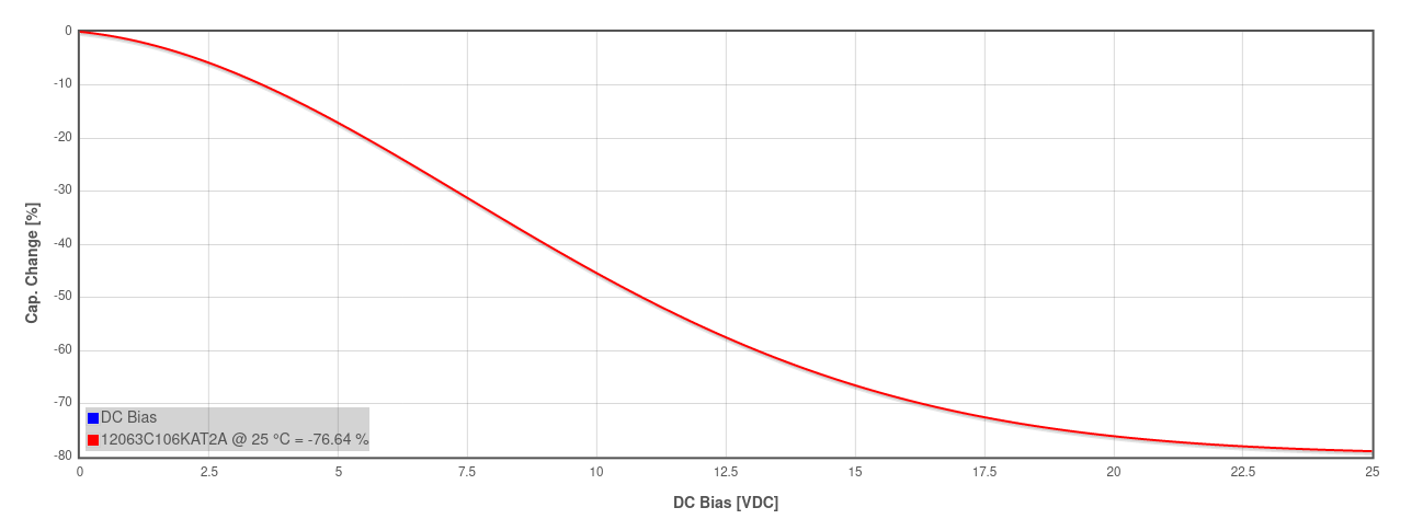
The capacitance of class 2 capacitors (such as X7R) falls as voltage is applied, meaning that the charging curve at a constant current won’t be linear, initially charging slowly then faster as the voltage increases. In addition to this, temperature has a significant effect on the capacitance.
As far as I’m aware, electrolytics and tantalum capacitors don’t have a significant variation of capacitance with applied voltage, but their wide tolerances and high leakages tend to make them only really suitable for decoupling.
Current Source
One of the most interesting parts of this project was designing the current source.
Basic Current Mirror
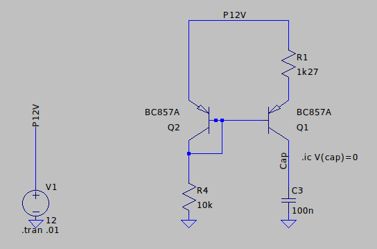
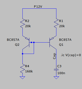
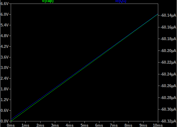
The first option I considered was a simple current mirror, with the reference provided by the fixed 12V supply across a resistor. Here, I resorted to simulation to help with the design.


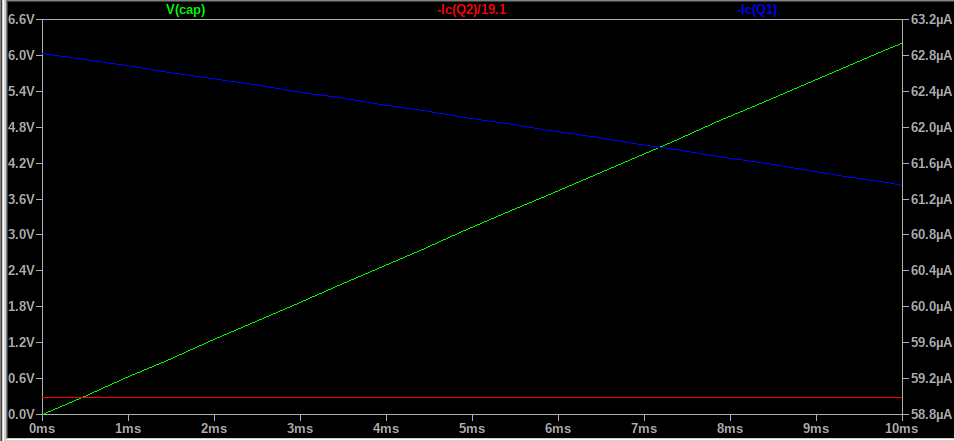
This works OK but you can see that the current mirror has an output impedance which is fairly significantly affecting the setpoint: around about 1Mohm. This gives a slightly nonlinear charging curve. The reason for this is the Early Effect, which essentially looks like a collector-emitter parallel impedance, sometimes referred to as hoe, ho or ro in the hybrid model.
Annoyingly, of the hybrid model parameters, the only one commonly specified in datasheets is hfe. I’ve never seen a datasheet which specifies Early voltage (which could be used to calculate hoe) and the datasheets for BC857 don’t even have the relevant curve to estimate it. The 1Mohm @ 60uA from the simulation though seems to suggest a ~60V Early voltage.
Widlar Mirror
The type of current source which I ended up choosing was the Widlar current source, although in hindsight this probably isn’t the best option.
The Widlar source augments the simple current mirror by adding an emitter degeneration resistor to the output transistor: this reduces the output current proportionally to exp(R1*Iout/vt) but also introduces some negative feedback to reduce the influence of the Early effect: as the output current reduces due to the Early effect, so the voltage across R1 will decrease, resulting in an increased base-emitter voltage, pushing the current back up. I’ve struggled to quantify this analytically despite this excellent article from analog (see section 11.8.2) but from this simulation, the impedance seems to have been increased to around 3.3Mohm:
One big weakness of this circuit is that there’s a significant effect of temperature on the current setpoint. The emitter degeneration resistor was selected based on a Vt of 25.8mV, which occurs at ~room temperature. As the temperature varies, the setpoint will vary. Let’s quantify this.
Temperature Variation
I first attempted to do this analytically, and found an interesting general result for Widlar current sources.
Referring to the schematic above, Vbe (=Vce) of Q2 will be given by:
 I_s ( e^{\frac{qV_{be,Q2}}{kT}} -1 )")
The exponential is the dominating term so to make the maths easier going forward, let’s ignore the -1 in the ebers-moll equation. Q1 is going to see a Vbe reduced by the voltage across R1:
}{kT}}")
Substituting one into the other and taking beta>>1 gives:

This is the result we quoted without derivation in the previous paragraph.
And differentiating wrt temperature, with the assumption that the R4 current is independent of temperature:
 e^{-\frac{q R1 I_o}{kT}}")
Factoring out the exponential:
")
Rearranging for dIo/dT gives the expression:
^2\right)}")
Plugging in the numbers gives dIo/dT = 225nA/K at 300K, or 0.4% per kelvin – not great but probably tolerable given the circuit will be working indoors and there’ll be little self-heating.
There’s one further incisive observation we can make of this expression. Provided the voltage across R1 is much greater than the thermal voltage (which will typically be the case for Widlar current source), this simplifies further to just Io/T. So a proportional variation in temperature of 1/T (so about 0.3% per Kelvin) is inherent in the design of a Widlar mirror. It seems odd then that it was used in integrated circuits, since I wouldn’t expect this to be acceptable.
Iterative Analysis
I also tried an iterative method to find the effect of temperature on output current, based on the method described on Wikipedia but assuming beta tends to infinity. I set up a spreadsheet to do a few levels of iteration, then compared the output current for 1K either side of 300K. This gave me a slightly different dIo/dT of around 149nA/K. I’m not quite sure what the source of the discrepancy is here, but I’m glad the numbers came out reasonably close.
Improved Mirror
An option I hadn’t considered until doing this write-up now, and which I wish I’d used, is this improved mirror circuit, which I can’t find a name for:
The “stilts” it’s standing on have the same effect on output impedance as in the Widlar source: as more current is drawn from Q1, the voltage drop across R1 increases, bringing the current back down.
Simulation indicates an output impedance of around 33Mohm.
It’s clear also from looking at this circuit that it won’t be significantly affected by temperature, since there should be no differential in Vbe between the two transistors. But how closely do we need to match R1 and R2? How sensitive is the circuit to the difference in the two? We would expect the gain to change as R1 and R2 vary.
Let’s assume nothing changes on the left hand side of the circuit and hfe tends to infinity. That means that the base voltage (relative to the positive supply) is fixed. I’ll call that VB. So the output current is given by:

Differentiating this and substituting Io back in to cancel out the scale current and beta gives:
\left( R1\frac{dI_o}{dR_1}+I_o \right)")
Rearranging gives:
}{1-\frac{I_oR_1}{v_t^2}\left(I_oR_1-V_B\right)}")
We could just plug numbers in now but we can make a useful observation if we look at the right hand side of the denominator. It has two parts: 


So, for as long as the assumption of R1 voltage being much greater than the thermal voltage applies, the output current just varies in proportion with the conductance of R1. This is unlike in the Widlar current source, where a change in resistance causes an exponential change in output current, giving the circuit high sensitivity to the value. This property of the improved current mirror would allow us to create a mirror with different ratios, with very little sensitivity to semiconductor parameters.
Wilkinson Mirror
A final type of current source which I won’t go into any detail here but which would also probably be an excellent choice for this circuit is the Wilkinson mirror – essentially the basic mirror but with a common-base amplifier to reduce the voltage variation seen by the mirror. Again, it’s described in this excellent source from Analog Devices.
Pulse Generator Circuit
Putting that all together, this is the pulse generator circuit:

Note that there’s no physical AND gate: since the comparators have open-drain outputs, tying them together with a pull-up resistor creates a wire-AND.
MOSFET Driving
Compared to other parts of the circuit, the MOSFET driving is relatively simple. What do we need in terms of switching time? To limit power dissipation, switching on fast is less important than switching off fast, since it will only be turning on near a transition when Vds will be low, whereas we might be turning off at any point in the mains cycle. Because of this, using the open-collector driver of the comparator and a pull-up is ideal. I chose 10k pull-up. Since the gate threshold voltage could be up to 4V, I’ve selected 12V as the power supply. This leaves 8V across the resistor. The pair of MOSFETs probably take around 200nC to switch (based on the datasheet for the similar IRF840), which means the switching time should be around 250us. Assuming (because we’re at a zero-crossing), drain voltage will be no more than 20V during a switch, and that the load will be up to 100mA, gives a turn-on dissipation of

The SN393T will pull down with a minimum of 6mA (like the LM393 which it imitates), so with a drain voltage now potentially as high as 325V, the turn-off dissipation is given by

This total dynamic dissipation of under 80mW (plus pretty negligible I²R losses) is low enough that I’m not even going to consider thermal management.
Power Supply
Earlier on in this project, I thought I might be able to get away with using under ~ a milliamp and so power the circuit with just a linear dropper from mains voltage. It turns out though, the total power consumption is a bit higher than that.
| Item | Current | Source |
| Comparators | 4mA | Datasheet max x2 parts |
| Current sources | 2.4mA | 12V/10k * 2 |
| Gate drive | 1.2mA | 12V/10k |
| Misc resistors | 1mA | Threshold circuits, inverters |
| Total | 8.85mA |
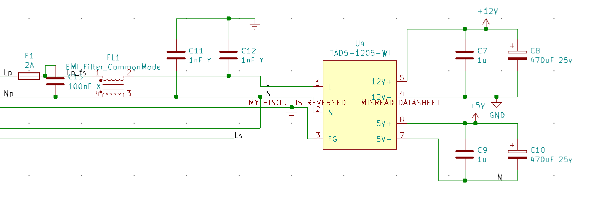
To produce the 8.85mA directly from 230V, I’d be dissipating at least 2W continuously. This isn’t acceptable for a dimmer. Instead, I decided to use this AC-DC power brick, which claims a no-load power consumption of <150mW.
It also has two outputs, isolated from one another.

I implemented it pretty much exactly as shown in the datasheet, including the EMI circuitry. While the FCC aren’t going to come hunting me down, I figured I probably ought to anyway!
Alternative Power Supplies
Before I realised the only sane option was a switched-mode power supply, I did a few experiments with other forms of power supply. Although I didn’t end up using any of the ideas I thought they might be worth sharing.
Zener Regulator
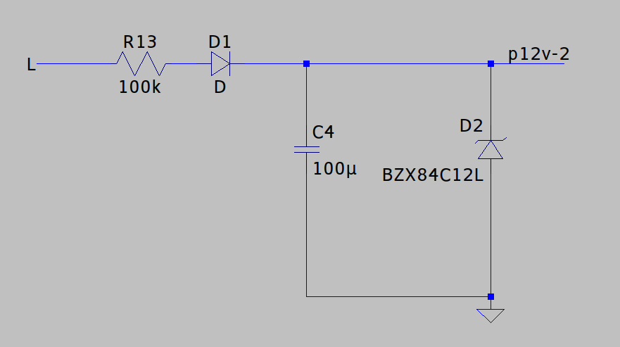
One of the simplest power supplies is just a rectifier and resistor to drop the voltage down from the mains supply, a zener to limit the voltage, and a capacitor to smooth it out. There are all kinds of problems with this: firstly, it’s no good here because unless we use a huge capacitor, there’ll be a lot of ripple – and none of the analog circuitry will thank us for that. The zener diode doesn’t regulate the voltage but rather clamps it, so the supply voltage will reach the zener voltage once per cycle, then droop.
The other problem is that these circuits are inherently power hungry: take the datasheet for BZX84C for example. For the <=24V parts, the test voltage is 5mA, which means you need at least 5mA through the diode to reach the zener voltage. Since that’s coming linearly from 230VAC, that’s 1.2W you’re burning just for the zener! As I understand it, this is one of the better zeners too.
You can get around this to some extent by using a shunt voltage regulator instead, such as TL432. This will work down to ~100uA and I’m working on another project at the moment which uses it. I’m starting to think that zener diodes are long overdue relegation to the history books – I’m struggling to think of any application where I’d choose one over a shunt regulator.
Another improvement you often see to this arrangement is replacing the resistor with a capacitor to improve efficiency: on one half of the mains cycle, the capacitor drops voltage by charging up, rather than burning power as a resistor would. On the other half of the cycle, the energy gets fed back into the mains supply. This is typically done in combination with a bridge rectifier but in this instance we might get away with just adding an antiparallel diode to discharge it:
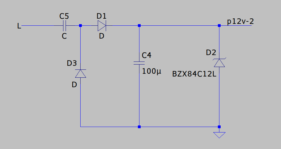
I haven’t looked into this in any great detail though and I’m not sure how exactly I’d model it/select the capacitor value. I’m also not sure how much you can gain from this, given that some resistance will be needed in series to limit the peak currents.
Linear Regulator
Linear regulators are typically limited to lower voltages, but there are a few linear regulators designed to work off mains voltage directly. One example is Microchip’s LR8, which can withstand input voltages of up to 450V. This is probably one of the best solutions for loads of ~2mA or less, but less suitable for this application. Again, this is something I’m looking into for another project so I’ll be writing some more detail on this in my (hopefully!) next post.
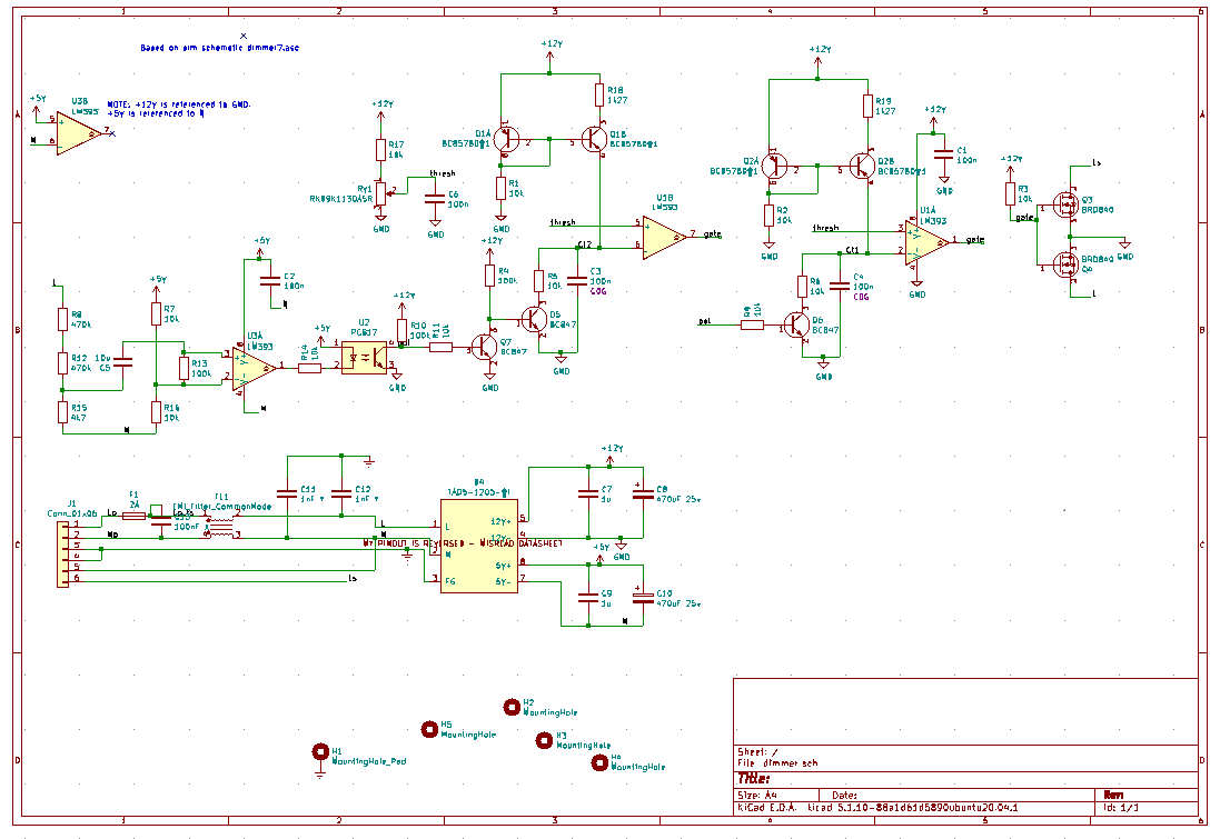
Completed Schematic and PCB Layout
Putting together my power supply, polarity detector, pulse generator and MOSFET, the schematic is complete.
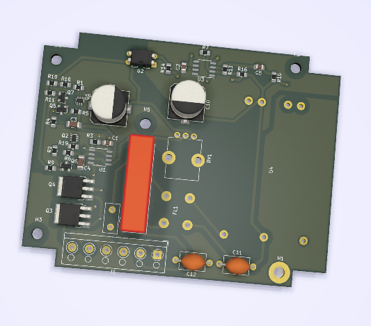
The PCB layout wasn’t too challenging, with the board having plenty of space:
KiCAD source files are here.
PCB Problems
Once the PCBs arrived and I started populating them: I ran into two problems. One was my fault and one was JLCPCB’s!
Firstly, I misread the datasheet for the AC-DC module. I’d misread the orientation of one of the drawings and my PCB footprint for the part was mirrored. I ended up having to mount it on the opposite side of the board : it’s lucky I didn’t have any tall components there!
The second problem was with the PCB manufacture. I was having problems with one of the current mirrors which I eventually narrowed down to one of the emitters of Q1 not being connected to +12V. I had to wiremod it to get the board to work!

It’s hard to see because of the silkscreen, even with a microscope, but the track/thermal which should connect the pad is completely missing.

In the gerber I sent them, it was definitely connected:

Test
The pulse generators produce a ramp very much as you’d expect:
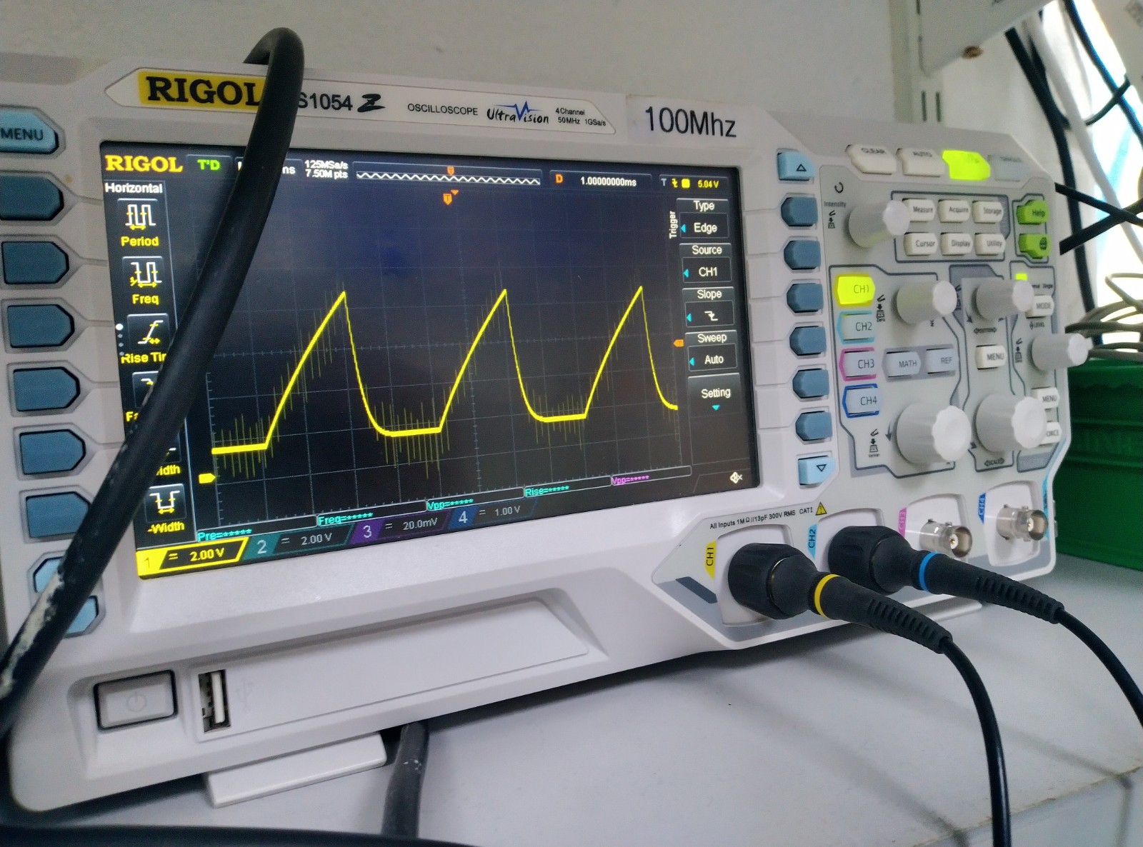
The charging curve isn’t as linear as I’d hoped, and the discharge is slower than I’d have liked. In hindsight, the discharge problem was due to a stupid decision on my part: I’m not sure why I chose 10k resistors, when 60uA*10k =600mV. It also gives a time constant of 1ms, which is a long time when the whole ramp is 10ms! I reduced the resistors to 1k, which seemed to improve it – I forgot to record a scope trace though!
Why is the ramp so nonlinear? It looks almost as if I oughtn’t have bothered with the current mirror at all. It looks like there’s some kind of parallel resistance. The comparator input bias current is very low so it shouldn’t be this. I considered that it might be flux on the PCB, but that’s typically in the megaohms, which shouldn’t be a problem here.
Despite this, the phase control seemed to work great:
The maximum phase is a bit off though because of the problems with the ramp generator, but in principle it seems to be working as expected.
Connecting this up to a lamp, I was a bit disappointed to find that the output was very flickery. Because of the rolling shutter/aliasing, the video makes it seem far worse than it does in real life. But it’s still not ideal. Even with an incandescent bulb, there’s a noticeable flicker.
I’m tempted to put this down to variation between the two pulse generators: since one works the positive half-cycle and the other works the negative half-cycle, any discrepancy between the two will cause a 50Hz flicker. And there are plenty of potential sources of discrepancy: the capacitors, while stable, are +/-5% starting tolerance. The emitter degeneration resistor in the current sources, to which the output current is superlinearly sensitive, are +/-1%. The circuit is also sensitive to the saturation voltage of the discharge transistors.
Conclusion
I think I’m going to conclude this project here and find some alternative solution for my lamp. A dimmer was a cool idea but maybe I don’t need one at all and a rotary switch will do?
It was interesting to dig a bit into the design and analysis of current sources, but I think I underestimated some of the subtleties of this project. If anything, it’s driven home the importance of doing tolerance analyses.
I hope this has made for interesting reading, and I welcome any comments, especially if you have any ideas what’s up with the nonlinearity of my ramp generator!